Yig Tuned Filters MA0326|3-31GHz| MA0350|3-50GHz| YTF
Custom frequency bands are available upon request.
Yig Tuned Filters MA0326|3-31GHz| MA0350|3-50GHz|
Yttrium Iron Garnet (YIG) is a crystal that has very high Q characteristics. This high Q provides very low phase noise in oscillators and multi-octave frequency tuning for both oscillators and filters.
The MA0326 is an ultra-wideband analog tunable filter designed based on the current-tuned Yttrium Iron Garnet (YIG) principle. It operates across a frequency range of 3 to 31 GHz with a typical 3dB bandwidth of 50 MHz. The out-of-band rejection under detuning is better than 80 dBc across the full frequency band, and its in-band flatness is superior to 1.5 dB. MA0350 operates across a frequency range of 3 to 50 GHz,drop-in replacement for Keysigh.
This component delivers high suppression against image frequencies and multiple spurious frequency responses. Additionally, it features excellent frequency selectivity, compact size, a wide operating temperature range and high tuning linearity. It can serve as a replacement for filter assemblies, making it an ideal option for test and measurement instruments as well as ultra-wideband receiver systems.YIG is a ferrite material that resonates at microwave frequencies when immersed in a DC magnetic field. This resonance is directly proportional to the strength of the applied magnetic field and has very linear
“tuning” over multi-octave microwave frequencies.
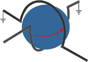
The DC magnetic field is generated using an electro-magnet, a permanent magnet, or a combination of both. The magnetic field of an electromagnet can be “tuned” using a variable current. Figure 1 illustrates a typical YIG filter magnet.
YIG crystal resonance is the alignment of external elec-tron paths at the molecular level (precession), creating a “combined” magnetic dipole: a magnetic field resonating at microwave frequencies around the YIG sphere.
Current generates magnetic fields, and magnet fields can generate current when coupled to a conductive “loop”. Using small conductive “loops” allows coupling to & from the YIG spheres resonant magnetic field
Bandpass Filters
Figure 2 illustrates typical coupling of YIG resonators in a single stage (sphere) bandpass filter. The coupling loops are aligned at a 90° angle to prevent direct RF coupling. One end of each loop is grounded. This prevents the fil-tered signal from being reflected.
The RF input signal of the coupling loop modulates the magnetic field around the YIG sphere, this modulation is coupled to the magnetic field resonating around the YIG sphere, which then couples to the second/output loop. The RF signal passing through the filter must be the same frequency as the RF magnetic field resonating around the YIG sphere.
The frequency bandwidth/spectrum that is coupled
through the YIG resonator is dependent on the spacing between the YIG resonator and the coupling loop. The closer the loop, the wider the bandwidth. Bandwidth can also be expanded by increasing the number of YIG resonators and carefully “tuning” the RF coupling loops. Filter insertion loss increases with expanded bandwidth.
A YIG bandpass filter’s 3 dB bandwidth expands as the filter is tuned to higher operating frequencies at a rate of approximately 20% per octave (e.g. 30 MHz @ 2 GHz, 50 MHz @ 18 GHz).
Micro Lambda’s standard YIG bandpass filter’s 3 dB bandwidth is 15 MHz to 40 MHz ( @ 2 GHz); 20 MHz to 50 Mhz ( @ 18 GHz). Filters with 3 dB bandwidths greater than 500 MHz are available above 6 GHz oper-ating frequency.
There is a limit (i.e. Limiting) on the total amount of RF energy that a YIG resonator/sphere can couple/
transfer (e.g. 0 dBm to +10 dBm).
Band Reject Filters – Signal Rejection
Figure 3 illustrates typical coupling of YIG resonators
in a two stage (sphere) band reject filter. There is only one coupling loop (ribbon) per YIG sphere. The cou-
pling loops are aligned along a straight line and are
interconnected between the YIG resonators.

The coupling loops are essentially RF transmission
lines that pass all RF energy. However, when these transmission lines are located close to the surface of the YIG sphere, the loop couples to the magnetic field resonating ( @ microwave frequencies ) around the YIG sphere.
This coupling essentially reflects/rejects in coming fre-quencies that are at the same RF frequency as the RF magnetic field resonating around the YIG sphere.
Rejection bandwidth is widened by increasing the num-ber of YIG resonators and carefully “tuning” the RF coupling loops.
Micro Lambda’s standard band reject filter’s 40 dB re-jection bandwidth is 15 MHz to 70 MHz.


